Semiconductor Packaging Equipment Guide: Technologies, Components, Processes and Applications
Semiconductor packaging equipment refers to the machines, tools, and supporting systems used to assemble, connect, protect, inspect, and test semiconductor devices after wafer fabrication. A finished chip is not normally used as an exposed piece of silicon. It needs a package that provides physical protection, electrical connections, heat management, and a practical interface with a circuit board or another electronic system.
Context
Semiconductor packaging equipment refers to the machines, tools, and supporting systems used to assemble, connect, protect, inspect, and test semiconductor devices after wafer fabrication. A finished chip is not normally used as an exposed piece of silicon. It needs a package that provides physical protection, electrical connections, heat management, and a practical interface with a circuit board or another electronic system.
The packaging stage has developed alongside the semiconductor industry. Early packages were relatively simple, while modern devices may use compact structures with many electrical connections and several layers. Semiconductor packaging equipment therefore covers a broad range of technologies, from die bonding and wire bonding to molding, inspection, thermal control, and electrical testing.
Main equipment categories
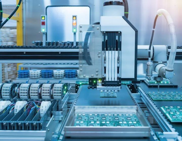
Common semiconductor packaging equipment includes die attach machines, wire bonders, flip-chip bonders, molding systems, package singulation machines, dispensing equipment, cleaning systems, optical inspection tools, X-ray inspection systems, and electrical test equipment. Material-handling systems are also important because chips and packages must move through several controlled steps without contamination or physical damage.
Importance
Semiconductor packaging affects how a chip connects with the rest of an electronic system. A package must maintain electrical connections while also dealing with mechanical stress, moisture, heat, vibration, and differences in thermal expansion between materials.
Modern electronics also require more compact and capable packages. This has increased interest in advanced packaging approaches such as 2.5D and 3D integration, chiplets, fan-out packaging, and high-density interconnect structures. These approaches can place greater demands on alignment, bonding, inspection, thermal management, and process control.
Why process control matters
Packaging involves many small steps, and each step can affect later stages. Examples include:
- Die placement must maintain accurate position and orientation.
- Bonding must create consistent electrical connections.
- Encapsulation must protect the device without introducing damaging stress.
- Singulation must separate packages without damaging edges or internal structures.
- Inspection must identify defects that may not be visible from the outside.
- Testing must verify electrical behavior under defined conditions.
Recent Updates
From 2024 through 2026, semiconductor packaging has received greater attention as chip designs have become more complex and as manufacturers have sought additional capacity outside established production centers. Advanced packaging is increasingly treated as an important part of the semiconductor supply chain rather than simply a final assembly step.
In India, government programs have supported the development of semiconductor fabrication, assembly, testing, packaging, equipment, materials, design, and related capabilities. The India Semiconductor Mission reports progress in OSAT and ATMP facilities, while government announcements in 2026 expanded the policy focus toward equipment and materials as part of the wider semiconductor ecosystem.
Semicon 2.0, approved in 2026, further emphasizes semiconductor equipment and materials, advanced packaging, research and development, design, fabrication, and talent development.
Technology trends
Several technology trends are shaping semiconductor packaging equipment:
- Advanced bonding: More precise bonding methods are being developed for dense interconnections and advanced package structures.
- Chiplet integration: Multiple smaller dies can be combined within one package, increasing requirements for placement, interconnection, and testing.
- 2.5D and 3D packaging: Vertical or closely integrated structures require accurate alignment and thermal planning.
- High-density inspection: Optical, X-ray, and other inspection methods help examine connections and internal structures.
- Automated handling: Equipment increasingly coordinates material movement, process recipes, inspection data, and production records.
- Thermal management: Packaging equipment and process design increasingly consider heat paths because high-performance chips can generate substantial heat.
Laws or Policies
Because the country was not specified, this section uses India as the policy context. Semiconductor packaging facilities in India can be affected by national semiconductor programs, environmental requirements, factory and workplace rules, electrical requirements, waste-management rules, and import or export controls that apply to particular equipment or materials.
The Semicon India Programme was established with a ₹76,000 crore outlay for developing the semiconductor and display manufacturing ecosystem. Government schemes cover areas including semiconductor fabs, display manufacturing, compound semiconductor facilities, ATMP or OSAT operations, and semiconductor design.
The Scheme for Promotion of Manufacturing of Electronic Components and Semiconductors, known as SPECS, was designed to support domestic manufacturing across identified electronic components, semiconductor or display facilities, specialized sub-assemblies, and certain capital goods. Its published framework includes plant, machinery, equipment, associated utilities, and technology within eligible capital expenditure categories.
The Electronics Component Manufacturing Scheme, notified in 2025, also includes supply-chain ecosystem and capital equipment among its target segments. This reflects a policy approach that considers equipment and component production part of the broader electronics manufacturing base.
Environmental and workplace requirements can also apply to packaging facilities. Depending on the materials and processes used, a facility may need to address chemical handling, emissions, hazardous waste, water use, electrical safety, worker protection, and electronic waste. Exact approvals depend on the facility, location, process, and substances involved, so applicable central and state requirements need to be checked for each project.
Tools and Resources
Readers researching semiconductor packaging equipment can use several technical and institutional resources to understand equipment categories, package structures, standards, and policy developments.
Useful resources
- India Semiconductor Mission: Provides information about India's semiconductor ecosystem, approved projects, and government programs.
- Ministry of Electronics and Information Technology: Publishes policy documents, scheme details, notifications, and program updates.
- JEDEC: Provides widely used semiconductor and electronics standards covering areas such as packages, memory, testing, and reliability.
- SEMI: Publishes industry standards and technical information related to semiconductor manufacturing equipment and materials.
- IPC: Develops standards and technical documents used across electronics manufacturing and assembly.
- Equipment specifications and process manuals: Manufacturer documentation can help readers understand machine functions, operating ranges, process steps, and maintenance requirements.
A simple equipment comparison table can help organize research:
| Equipment | Main process | Typical purpose |
|---|---|---|
| Die attach machine | Die placement | Positions and attaches semiconductor dies |
| Wire bonder | Wire bonding | Connects die pads to package connections |
| Flip-chip bonder | Flip-chip assembly | Places and connects dies using bumps |
| Molding system | Encapsulation | Protects the package structure |
| Singulation system | Package separation | Separates individual packages |
| Optical inspection | Visual inspection | Detects visible alignment and surface defects |
| X-ray inspection | Internal inspection | Examines hidden connections and structures |
| Test handler | Device handling | Moves devices through electrical testing |
| Thermal system | Heat management | Controls or evaluates package temperature |
FAQs
What is semiconductor packaging equipment?
Semiconductor packaging equipment includes machines used to attach dies, create electrical connections, encapsulate packages, separate units, inspect assemblies, and test finished devices. The exact equipment depends on the package technology and production process.
What are the main types of semiconductor packaging equipment?
Common types include die attach machines, wire bonders, flip-chip bonders, molding systems, singulation equipment, dispensing systems, inspection tools, and test handlers. Advanced facilities may also use equipment for specialized bonding and high-density package assembly.
How does advanced packaging change equipment requirements?
Advanced packaging can require tighter alignment, more controlled bonding, greater inspection capability, improved thermal management, and more complex testing. Technologies such as chiplets and 3D integration can increase the number of process interactions within a package.
What is the role of OSAT and ATMP in semiconductor packaging?
OSAT means outsourced semiconductor assembly and test. ATMP refers to assembly, testing, marking, and packaging. Both describe parts of the semiconductor back-end manufacturing chain where packaging and testing activities are carried out.
What policies support semiconductor packaging in India?
India's semiconductor policy framework includes the Semicon India Programme and related schemes supporting semiconductor manufacturing, packaging, design, equipment, materials, and components. Policy details can change, so current information should be checked through official government sources.
Conclusion
Semiconductor packaging equipment supports the transition from fabricated semiconductor dies to protected, tested, and usable electronic components. The equipment covers bonding, molding, singulation, inspection, handling, thermal management, and electrical testing. From 2024 through 2026, advanced packaging, chiplet integration, and domestic semiconductor capacity have received increasing attention, including in India. Understanding the equipment together with package design, process control, materials, standards, and applicable regulations provides a clearer view of how modern semiconductor packaging works.