Explore Semiconductor Manufacturing With Modern Fabrication Techniques and Technical Details
Semiconductor manufacturing is the process of turning specially prepared materials, usually silicon wafers, into integrated circuits that perform computing, sensing, communication, memory, and control functions. These tiny circuits are found in smartphones, computers, vehicles, industrial equipment, medical electronics, communication systems, and many other digital products.
Modern semiconductor manufacturing combines chemistry, physics, materials science, precision engineering, software, and automated inspection. A semiconductor fabrication facility, commonly called a fab, works in highly controlled environments because microscopic particles can affect circuit patterns that are much smaller than the width of a human hair.
The semiconductor fabrication process generally begins with a silicon wafer. Manufacturers repeatedly create, modify, remove, and inspect extremely thin layers of material. Techniques such as photolithography, deposition, etching, ion implantation, cleaning, and chemical-mechanical planarization are used to create transistor structures and electrical connections.
The overall process can be divided into several major stages:
- Wafer preparation involves producing and polishing semiconductor wafers.
- Patterning transfers circuit designs onto wafer surfaces.
- Deposition adds controlled layers of material.
- Etching removes selected portions of those layers.
- Doping changes the electrical characteristics of semiconductor regions.
- Metallization creates electrical connections between circuit elements.
- Inspection and testing identify defects and verify performance.
- Packaging protects the finished die and provides electrical connections.
These steps may be repeated many times. Semiconductor manufacturing therefore depends on precise process control rather than a single manufacturing operation.
From Silicon to Integrated Circuits
Silicon is widely used because its electrical properties can be controlled through carefully engineered processes. A polished wafer provides the foundation on which microscopic transistor structures are constructed.
Photolithography is particularly important. In this process, light is used to transfer selected patterns from a mask onto a photosensitive material called photoresist. Advanced fabrication techniques can use sophisticated lithography systems to create increasingly detailed patterns.
The patterned wafer then moves through processes such as etching and deposition. Each cycle modifies specific areas while preserving others, gradually building the architecture of the integrated circuit.
Importance
Semiconductor manufacturing matters because modern digital infrastructure depends on integrated circuits. Computing devices, communication equipment, transportation systems, industrial controllers, sensors, and data-processing infrastructure all rely on semiconductor components.
For everyday users, semiconductor production influences the capabilities of electronic products. Processor performance, memory capacity, energy efficiency, connectivity, and sensor functions are all connected to semiconductor technology.
For manufacturers, one major challenge is controlling defects. A small particle, variation in layer thickness, temperature change, or chemical imbalance can affect a microscopic structure. Production therefore requires monitoring systems that can detect process variation before it affects large numbers of wafers.
Why Fabrication Precision Matters
Modern chips contain enormous numbers of individual electrical elements. Their dimensions and spacing must remain within carefully controlled process limits.
Important manufacturing requirements include:
- Extremely clean production environments
- Accurate temperature and humidity control
- Precise chemical handling
- Stable equipment operation
- Automated process monitoring
- Microscopic defect inspection
- Consistent wafer processing
- Reliable electrical testing
Another important factor is yield. Yield describes the proportion of manufactured units that meet defined specifications. Improving yield requires identifying the causes of defects and controlling process variation across different manufacturing stages.
Major Semiconductor Manufacturing Stages
| Manufacturing Stage | Main Purpose | Common Technologies |
|---|---|---|
| Wafer preparation | Create a clean semiconductor foundation | Polishing, cleaning |
| Lithography | Transfer circuit patterns | Photolithography, advanced lithography |
| Deposition | Add material layers | CVD, PVD, ALD |
| Etching | Remove selected materials | Dry and wet etching |
| Doping | Modify electrical properties | Ion implantation |
| Planarization | Flatten wafer surfaces | CMP |
| Metallization | Create electrical pathways | Conductive deposition |
| Inspection | Identify defects | Optical and electronic inspection |
| Packaging | Protect and connect the die | Die attach, bonding, advanced packaging |
Recent Updates
From 2024 through 2026, semiconductor manufacturing has increasingly focused on supply-chain resilience, advanced packaging, artificial intelligence hardware, energy efficiency, and domestic fabrication capabilities.
One important development has been the expansion of semiconductor ecosystems beyond traditional wafer fabrication. Packaging and testing facilities have received increased attention because advanced packaging can connect multiple dies and support applications such as high-performance computing and artificial intelligence.
India has also expanded its semiconductor manufacturing ecosystem through the India Semiconductor Mission. Official programme information describes support for semiconductor fabs, compound semiconductor facilities, sensors, silicon photonics, packaging and testing facilities, and semiconductor design.
The government has reported progress involving fabrication, assembly, testing, marking, packaging, and design activities. The Semiconductor Laboratory in Mohali is also undergoing modernization, with an emphasis on an 8-inch 180 nm CMOS fabrication line and improved operational capabilities.
Advanced Packaging
Advanced packaging has become increasingly important because improving chip performance is not limited to reducing transistor dimensions. Engineers can also improve system performance by placing multiple semiconductor dies together within a package.
Approaches include chiplet architectures, 2.5D packaging, 3D integration, flip-chip connections, wafer-level packaging, and high-density interconnects.
These technologies can help designers combine different types of processing, memory, and specialized functions within a single system.
Automation and Process Monitoring
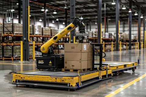
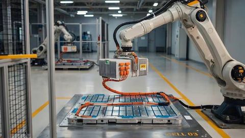
Modern semiconductor fabrication facilities rely heavily on automated equipment and digital monitoring. Sensors collect information about temperature, pressure, chemical conditions, vibration, particle levels, and equipment performance.
Data analysis can then identify unusual process conditions. This supports preventive maintenance, defect analysis, process optimization, and production consistency.
Laws or Policies
In India, semiconductor manufacturing is shaped by national electronics and semiconductor programmes administered through the Ministry of Electronics and Information Technology and the India Semiconductor Mission.
The Modified Programme for Development of Semiconductors and Display Manufacturing Ecosystem has an approved outlay of ₹76,000 crore. Its components include schemes for semiconductor fabs, display fabs, compound semiconductors and packaging facilities, along with the Design Linked Incentive scheme.
The semiconductor fab scheme provides fiscal support of up to 50% of eligible project expenditure on a pari-passu basis for approved projects. The related compound semiconductor, silicon photonics, sensor, and semiconductor packaging scheme provides support linked to capital expenditure.
Policy also covers semiconductor design. The Design Linked Incentive programme supports eligible semiconductor design activities across development and deployment stages, connecting chip architecture and intellectual property development with the wider manufacturing ecosystem.
Other electronics manufacturing policies can also affect the broader semiconductor supply chain. SPECS, for example, was created to strengthen domestic manufacturing of electronic components and semiconductor-related equipment and materials.
These policies are part of a broader effort to develop capabilities across design, fabrication, assembly, testing, packaging, research, and technical skills.
Tools and Resources
Understanding semiconductor manufacturing can involve several categories of technical tools and learning resources.
Semiconductor Design Tools
Electronic design automation software is used to create and verify integrated circuit designs. These tools support activities such as circuit simulation, physical design, verification, layout, and timing analysis.
Process Simulation
Process and device simulation tools help engineers study how fabrication steps affect semiconductor structures and electrical behavior. Simulation can be useful before experimental manufacturing because it allows engineers to evaluate process parameters and device characteristics.
Metrology and Inspection
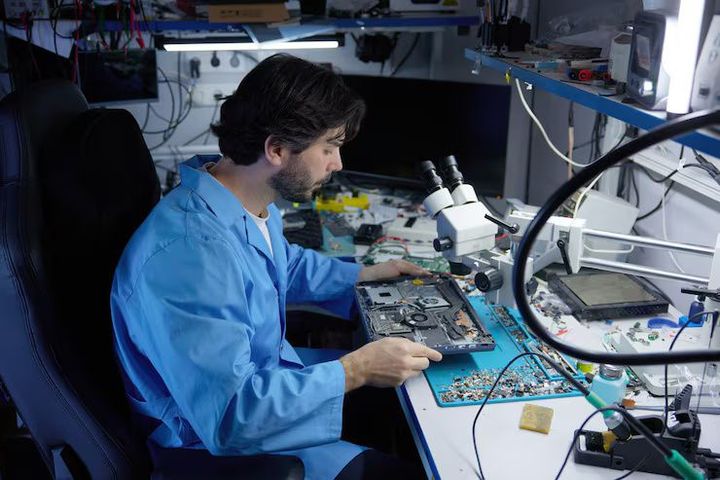
Metrology equipment measures physical characteristics such as layer thickness, critical dimensions, surface properties, alignment, and material characteristics. Inspection systems can identify microscopic defects across wafer surfaces.
Public Technical Resources
Government semiconductor programme portals, technical institutes, semiconductor research publications, equipment documentation, standards organizations, and university learning materials can help readers understand semiconductor fabrication process concepts.
For beginners, a useful learning sequence is silicon fundamentals, transistor operation, wafer processing, photolithography, deposition, etching, doping, interconnects, testing, and packaging.
FAQs
What is semiconductor manufacturing?
Semiconductor manufacturing is the controlled production of integrated circuits on semiconductor wafers. It includes wafer preparation, patterning, deposition, etching, doping, metallization, inspection, testing, and packaging.
What are modern fabrication techniques?
Modern fabrication techniques include advanced photolithography, atomic layer deposition, chemical vapor deposition, plasma etching, ion implantation, chemical-mechanical planarization, advanced metrology, and sophisticated packaging technologies.
How does semiconductor fabrication work?
Semiconductor fabrication works through repeated cycles of adding, patterning, modifying, removing, and inspecting extremely thin material layers on a wafer. These cycles gradually create transistors and electrical connections.
Why is wafer fabrication important in semiconductor manufacturing?
Wafer fabrication creates the physical structures that form integrated circuits. Precise control of each wafer fabrication step is necessary because microscopic variations can affect circuit performance and manufacturing yield.
What is semiconductor packaging?
Semiconductor packaging places a completed semiconductor die into a protective structure and creates electrical connections between the die and the larger electronic system. Advanced packaging can also integrate multiple dies within one package.
Conclusion
Semiconductor manufacturing combines materials science, precision engineering, chemistry, electronics, automation, and computer-controlled processes. Modern fabrication techniques allow manufacturers to create increasingly complex circuits through repeated wafer-processing stages. Recent developments have expanded attention toward advanced packaging, process automation, artificial intelligence hardware, and semiconductor ecosystem development. In India, government programmes now cover multiple parts of the semiconductor value chain, including fabrication, packaging, testing, design, and research.