Semiconductor Wafer Processing Machines: Silicon Carbide Technology Explained
Semiconductor technology is an important part of modern electronics. It supports equipment used in electric vehicles, renewable energy systems, industrial automation, telecommunications, and power management. As these applications develop, manufacturers need semiconductor materials that can operate efficiently under demanding electrical and thermal conditions.
Silicon carbide, commonly known as SiC, is a semiconductor material made from silicon and carbon. Compared with conventional silicon, it can withstand higher electric fields and operate at higher temperatures. It also has useful thermal properties that help electronic devices manage heat.
These characteristics make silicon carbide particularly valuable for power electronics, where components control or convert electrical energy.
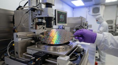
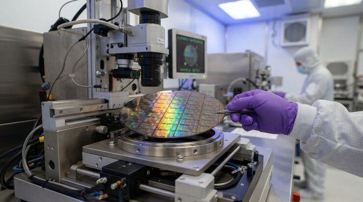
Semiconductor wafer processing machines are specialized systems used to prepare, shape, clean, inspect, and modify semiconductor wafers. A wafer is a thin, flat disc that serves as the foundation for manufacturing electronic devices.
Silicon carbide wafers require careful processing because the material is hard, chemically stable, and sensitive to certain manufacturing defects. Its properties make some processing operations more demanding than comparable operations involving ordinary silicon.
The manufacturing process combines several stages, including wafer preparation, surface polishing, cleaning, lithography, etching, material deposition, doping, and inspection. Each stage helps create the precise structures needed for reliable semiconductor devices.
How Silicon Carbide Technology Works
Silicon carbide technology relies on the material's wide bandgap and high breakdown electric field. These properties help designers develop power devices that can handle high voltages and switching frequencies.
Common SiC components include:
Power MOSFETs: Electronic switches used to control electrical power.
Schottky diodes: Components that allow current to flow primarily in one direction.
Power modules: Assemblies containing semiconductor components for larger electrical systems.
High-voltage devices: Components designed for demanding power conversion applications.
The performance of these devices depends on more than the raw material. Wafer quality, crystal defects, surface finish, contamination control, and manufacturing precision all influence the final result.
Main Types of Semiconductor Wafer Processing Machines
Different machines are used at different stages of SiC semiconductor manufacturing. Each system performs a specific task and must meet strict requirements for precision, cleanliness, and repeatability.
Machine type | Main purpose |
|---|---|
Wafer slicing equipment | Cuts semiconductor crystals into thin wafers |
Grinding and lapping machines | Control wafer thickness and surface geometry |
Chemical mechanical polishing systems | Produce smooth, uniform wafer surfaces |
Wafer cleaning equipment | Removes particles and chemical residues |
Lithography systems | Transfer circuit patterns onto wafer surfaces |
Plasma etching machines | Remove selected material to create device structures |
Epitaxy systems | Grow controlled semiconductor layers |
Ion implantation systems | Introduce selected impurities into semiconductor material |
Inspection and metrology systems | Measure dimensions and identify defects |
Wafer testing equipment | Evaluates electrical characteristics at appropriate production stages |
The equipment used depends on the product, manufacturing process, wafer diameter, and required quality level. Not every production line uses identical equipment or follows exactly the same sequence.
The Silicon Carbide Wafer Manufacturing Process
SiC wafer production begins with crystal growth and continues through wafer preparation and device fabrication. Maintaining consistent quality throughout this sequence is essential.
Crystal growth and wafer preparation
Manufacturers first grow silicon carbide crystals using controlled temperature and environmental conditions. The resulting crystal, often called a boule, is prepared for slicing.
Specialized cutting equipment separates the crystal into thin wafer sections. Because silicon carbide is extremely hard, cutting requires careful control to limit material damage and unwanted surface irregularities.
Grinding, lapping, and polishing
After slicing, wafers may contain surface damage, uneven thickness, or microscopic irregularities. Grinding and lapping help correct these issues.
Chemical mechanical polishing combines chemical reactions with mechanical movement to create a smoother surface. This stage is particularly important when preparing wafers for subsequent semiconductor processing.
Cleaning and contamination control
Even small particles can interfere with device formation. Wafer cleaning systems remove unwanted residues using carefully controlled chemical or physical methods.
Cleanroom procedures also help limit contamination from airborne particles, equipment contact, and materials used during production.
Epitaxial layer growth
Epitaxy creates a controlled crystalline layer on the wafer surface. In SiC manufacturing, this layer can be designed with specific electrical properties required for the intended device.
Chemical vapor deposition is commonly used for this purpose. Process conditions influence layer thickness, uniformity, and defect formation.
Patterning, etching, and doping
Lithography defines patterns that guide later manufacturing operations. Etching removes selected material, while doping introduces controlled impurities to modify electrical behavior.
These operations create the structures needed for semiconductor devices. The exact sequence varies according to the device design and manufacturing technology.
Inspection and electrical testing
Inspection systems identify surface defects, particles, and dimensional variations. Electrical testing helps determine whether devices behave as expected.
Manufacturers use this information to improve process control and identify recurring production problems.
Importance of Silicon Carbide Processing Technology Today
Silicon carbide has become important because many electrical systems require efficient power conversion, high-voltage operation, and reliable performance under demanding conditions.
Its value extends across several industries.
Electric vehicles: SiC power devices can support traction inverters, onboard charging systems, and charging infrastructure.
Renewable energy: Solar inverters and other power conversion equipment can use SiC components to manage electrical energy.
Industrial automation: Motor drives, power supplies, and control equipment may benefit from high-performance power semiconductors.
Energy infrastructure: Electrical conversion and distribution systems use power devices to regulate voltage and current.
Telecommunications: Power management systems can incorporate advanced semiconductor components to support electronic infrastructure.
For manufacturers, precise wafer processing helps control defects, maintain consistent electrical properties, and improve device reliability. For engineers, it provides a foundation for designing components that meet specific operating requirements.
However, silicon carbide is not automatically the best choice for every application. Conventional silicon remains suitable for many products, while other wide-bandgap materials may be better suited to particular switching or frequency requirements.
Challenges in Silicon Carbide Wafer Processing
Although SiC has useful physical properties, manufacturing it presents several technical challenges.
Material hardness: Silicon carbide is difficult to cut and polish. Processing equipment must balance removal rates with surface quality.
Crystal defects: Defects formed during crystal growth or later processing can affect device performance and manufacturing yield.
Surface damage: Improper slicing or grinding can create subsurface damage that requires additional processing to remove.
Contamination: Particles, metals, and chemical residues can interfere with sensitive fabrication steps.
Process consistency: Variations in temperature, pressure, gas flow, chemical concentration, or equipment condition can affect wafer quality.
Measurement accuracy: Manufacturers need reliable methods to measure thickness, flatness, surface roughness, and defect density.
Process monitoring, preventive maintenance, and statistical quality control help address these challenges. The appropriate method depends on the specific production stage and device requirements.
Recent Developments and Industry Trends
During 2025 and 2026, semiconductor manufacturing continued to evolve in response to demand for power electronics, artificial intelligence infrastructure, electric mobility, and more resilient supply chains.
Several developments are relevant to silicon carbide wafer processing.
Larger wafer formats: Manufacturers are working to expand the use of 200 mm silicon carbide wafers alongside established 150 mm production. Larger wafers can provide more usable area per wafer, although production benefits depend on yield, equipment compatibility, and process maturity.
Greater automation: Automated wafer handling, process monitoring, and equipment data collection help reduce unnecessary manual contact and improve repeatability in controlled manufacturing environments.
More attention to equipment and materials: On July 15, 2026, India's Union Cabinet approved Semicon 2.0, with a reported total outlay of ₹1,27,500 crore. The programme includes semiconductor equipment, materials, fabrication, research, and workforce development among its priorities. This creates a broader policy focus on the supporting technologies needed for domestic semiconductor manufacturing.
These trends do not mean every factory has adopted the same technologies. Implementation depends on manufacturing requirements, technical readiness, infrastructure, and investment priorities.
Laws, Policies, and Manufacturing Standards
Semiconductor manufacturing operates under national regulations and technical standards. The exact requirements depend on the country, facility, production processes, and materials handled.
In India, several policy areas are relevant.
India Semiconductor Mission: The Semicon India Programme supports the development of semiconductor fabrication, compound semiconductor facilities, chip design, and packaging infrastructure. Its policy framework aims to strengthen domestic manufacturing capabilities. Individual projects must satisfy the applicable scheme requirements to receive support.
Occupational safety: Workers handling high-temperature equipment, chemicals, vacuum systems, and industrial gases require appropriate training, protective equipment, and documented safety procedures.
Technical standards: Standards covering equipment safety, cleanroom performance, measurement methods, and quality management can help manufacturers establish consistent operating practices. Applicable standards should be selected according to the facility and its processes.
Regulatory obligations can change, so manufacturers should verify current requirements with qualified compliance professionals and the relevant authorities before establishing or modifying a production facility.
Tools and Resources for Learning and Process Control
General-purpose technical tools can help students, engineers, and manufacturing teams understand silicon carbide wafer processing.
Process flow diagrams: Map the sequence of wafer slicing, polishing, cleaning, fabrication, and testing.
Statistical process control software: Tracks manufacturing variation and helps identify unusual process behavior.
Surface metrology instruments: Measure roughness, flatness, thickness, and other physical characteristics.
Optical inspection systems: Detect visible surface irregularities and selected wafer defects.
Electrical characterization instruments: Measure properties such as resistance, voltage response, and current behavior.
Equipment maintenance logs: Record calibration, inspections, component replacement, and maintenance activities.
Process simulation tools: Help engineers examine manufacturing parameters before applying changes in a production environment.
Technical training materials: Explain semiconductor physics, cleanroom practices, materials science, and equipment operation.
When evaluating a processing system, manufacturers should consider wafer diameter, material compatibility, throughput requirements, process repeatability, contamination controls, maintenance needs, and measurement capability.
Frequently Asked Questions
What are semiconductor wafer processing machines?
These are specialized machines used to prepare and manufacture semiconductor wafers. They perform operations such as cutting, polishing, cleaning, patterning, etching, layer deposition, inspection, and testing.
Why is silicon carbide used in power electronics?
Silicon carbide has a wide bandgap, a high breakdown electric field, and useful thermal properties. These characteristics make it suitable for many high-voltage and high-temperature power conversion applications.
How is SiC wafer processing different from silicon processing?
SiC is harder and more chemically stable than silicon, making wafer cutting and polishing more demanding. Its crystal growth and fabrication processes also require material-specific controls and equipment settings.
What industries use silicon carbide semiconductor devices?
Common applications include electric vehicles, renewable energy systems, industrial motor drives, charging infrastructure, and power management equipment.
What should manufacturers consider when selecting wafer processing equipment?
Important factors include wafer size, surface quality, defect detection, material compatibility, process repeatability, automation capability, safety requirements, and maintenance planning.
Conclusion
Semiconductor wafer processing machines play a central role in turning silicon carbide material into reliable electronic components. Each manufacturing stage contributes to wafer quality, from crystal preparation and polishing to advanced fabrication and electrical testing.